Terminal and contact stamping is a critical manufacturing process for electrical connectors, power distribution assemblies, electronics, sensors, controls and EV battery systems. Metalstampingparts.ltd supports B2B buyers that need custom stamped terminals, connector contacts, spring contacts, battery tabs, busbar-related terminals and precision conductive components made to drawing.
As a metal stamping parts manufacturer, we focus on practical manufacturability, stable production quality and application-specific material selection. Whether you are sourcing a new connector program or replacing an unstable terminal supplier, our team can review drawings, material specifications, plating requirements, annual volume targets and inspection expectations before production begins.
Projects commonly involve copper alloy, brass and phosphor bronze terminals produced with progressive die stamping, compound tooling or secondary forming operations. For buyers comparing a connector terminal progressive die stamping supplier, a copper progressive die stamping terminals supplier or a precision stamped contacts manufacturer, the goal is not only a stamped shape; it is a reliable electrical interface that fits, conducts and performs consistently in assembly.
Custom Stamped Terminals and Electrical Contacts
Terminals and contacts are small parts with large consequences. A minor burr, unstable bend angle, poor flatness, incorrect spring force or inconsistent plating area can create insertion problems, contact resistance changes, overheating, loose connection or assembly downtime. Our production approach starts from the functional requirements of the component: mating interface, current path, retention method, spring behavior, crimping area, soldering area, plating surface and downstream assembly process.
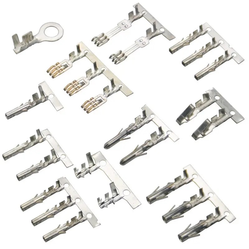
We support OEMs, contract manufacturers, connector companies and industrial buyers that need made-to-print stamped parts rather than catalog terminals. Typical designs include male and female connector terminals, blade terminals, fork terminals, receptacle contacts, lead frame style contacts, battery connector contacts, shield clips, grounding contacts, EMI contacts, relay contacts and small spring contact components.
If your program is related to electrical assemblies, you may also find our broader electrical metal stamping capabilities useful for brackets, conductive clips, shields and precision electrical hardware.
Progressive Die Stamping for Connector Terminals
High-volume terminal production often depends on progressive die stamping because multiple cutting, piercing, coining, embossing and forming stations can be integrated into one continuous strip process. This is especially useful for connector terminals where part geometry is thin, detailed and repeatability-sensitive. A well-designed progressive die can control pitch, carrier design, bend sequence, pilot positioning and feature consistency across production lots.
As a connector terminal progressive die stamping supplier, we evaluate strip layout early to reduce unnecessary material waste and improve forming stability. For thin conductive materials, die clearance, punch sharpness, feed accuracy and carrier strength are important to manage burr height, distortion and feature repeatability. When needed, terminals may remain connected to a carrier strip for reel-to-reel handling, automated plating or automated assembly.
For more information about this production method, see our progressive die stamping service page.
Materials for Terminal and Contact Stamping
Material selection affects conductivity, formability, spring properties, corrosion resistance, mechanical strength and cost. Buyers often specify copper, brass or phosphor bronze according to the electrical load, mating cycles, environmental conditions and mechanical retention requirements. If a drawing already defines the exact alloy and temper, we manufacture according to that specification. If a program is still in development, we can discuss common stamping considerations so your engineering team can confirm the final selection.
| Material | Typical Use in Terminals and Contacts | Key Stamping Considerations |
|---|---|---|
| Copper and copper alloys | Conductive terminals, battery tabs, grounding contacts, power connector components and low-resistance current paths. | Excellent conductivity; requires attention to softness, burr control, deformation and plating compatibility. |
| Brass | Connector terminals, crimp terminals, electrical clips, contact blades and general conductive stamped parts. | Good balance of conductivity, strength, formability and cost; commonly used for medium-duty terminals. |
| Phosphor bronze | Spring contacts, connector contact beams, retention clips and components requiring elastic performance. | Useful for spring behavior and fatigue resistance; bend radius and grain direction should be reviewed carefully. |
| Stainless steel or nickel alloy options | Shielding contacts, spring clips, battery hardware or special environmental applications where conductivity is secondary. | Higher forming force and springback may require dedicated tooling and additional dimensional control. |
For material-specific pages, visit copper stamping and brass stamping. If you need a connector phosphor bronze spring contacts supplier, please include the material grade, temper, thickness and expected spring function with your RFQ.
Applications We Support
Terminal and contact stamping serves many industries where electrical performance and repeatable assembly are required. We manufacture custom stamped contacts and terminals for both signal-level and power-related applications, depending on the drawing, material and tolerances.
- Connectors: male terminals, female receptacles, contact beams, retention features, shields and grounding clips.
- Electronics: PCB contacts, battery contacts, sensor contacts, relay components and small conductive brackets.
- EV and energy systems: battery module terminals, conductive tabs, busbar-related stamped details and power connection components.
- Industrial controls: switch contacts, fuse contacts, relay terminals, grounding contacts and control cabinet components.
- Automotive and mobility: connector terminals, clips, sensor terminals and electrical interface components used in assemblies.
- Appliances and equipment: power terminals, spring contacts, grounding elements and stamped electrical hardware.
Buyers searching for an EV battery precision stamped terminals supplier should provide current rating assumptions, material requirements, plating expectations, assembly method and any thermal or vibration considerations. We do not replace your engineering validation, but we can manufacture the stamped component to the agreed drawing and inspection plan.
For electronics-related applications, see our electronics industry page.
Design and Manufacturability Review
Before tooling, our team reviews the drawing for manufacturability and production risk. Important factors include material thickness, feature spacing, bend radius, forming direction, flatness requirements, burr direction, plating mask area, carrier requirements and packaging method. For contact parts, we also pay attention to spring arms, coined contact points, insertion zones and mating surfaces because these areas directly affect function.
Common terminal stamping issues include excessive burrs near the mating edge, cracks at tight bends, unstable formed angles, distorted thin sections, inconsistent crimp wings and contact surface damage. If your current parts have recurring production problems, our guide to electrical terminal stamping issues may help identify possible causes before you send a new RFQ.
For tight-tolerance programs, see our precision metal stamping capabilities. Precision does not mean every feature needs the tightest possible tolerance; it means the critical features are clearly defined, measurable and controlled during production.
Quality Control for Stamped Contacts and Terminals
Quality control for terminal and contact stamping must be built into the process, not added only at final inspection. The control plan may vary by part complexity and buyer requirements, but typical checks include material verification, first article inspection, in-process dimensional checks, burr direction review, flatness checks, bend angle checks, pitch and carrier inspection, visual surface inspection and packaging verification.
For contact components, important inspection points may include contact width, tab thickness, formed height, gap, spring arm geometry, crimp area dimensions, hole position, slot width and plating-sensitive surfaces. Depending on the application, additional inspection may include functional go/no-go gauges, insertion fit checks or customer-defined measurement points.
We encourage buyers to define critical-to-function dimensions on the drawing. This helps align tooling, inspection frequency and documentation with the actual risk areas of the part. If PPAP, first article reports, material certificates or special inspection records are required, please state those needs during the RFQ stage so they can be included in the production plan.
RFQ Information That Helps Us Quote Faster
To receive a practical quotation for terminal and contact stamping, please provide as much of the following information as possible:
- 2D drawing and 3D model if available
- Material grade, thickness and temper
- Plating type, plating area and any masking requirements
- Annual volume, order quantity and expected production schedule
- Critical dimensions and inspection documentation requirements
- Packaging preference, such as bulk, tray, tube, reel or carrier strip
- Application background, especially for connector, EV battery or spring contact parts
This information helps us evaluate whether progressive die stamping, single-operation tooling or a staged development approach is most suitable for your project.
FAQ: Terminal and Contact Stamping
What is terminal and contact stamping?
Terminal and contact stamping is the process of producing conductive electrical interface components from metal strip or sheet using stamping dies. The process may include blanking, piercing, coining, embossing, bending, forming and carrier strip design for automated handling.
Can you stamp copper terminals?
Yes. We manufacture copper and copper alloy stamped terminals according to customer drawings. Copper is often selected for conductivity, but the design must account for softness, forming behavior and surface protection. Buyers looking for a copper progressive die stamping terminals supplier should include alloy, temper and plating details in the RFQ.
Can you produce brass connector terminals?
Yes. Brass is widely used for stamped connector terminals because it offers a practical balance of conductivity, formability, mechanical strength and cost. If you need a brass progressive die stamping terminals supplier, we can review your drawing and production volume to determine the appropriate tooling approach.
Do you manufacture phosphor bronze spring contacts?
Yes, we can manufacture stamped phosphor bronze spring contacts to drawing. Phosphor bronze is commonly selected where spring behavior and fatigue resistance are important. Bend geometry, material temper and grain direction should be reviewed carefully.
Can terminals be supplied on a carrier strip?
Many terminal designs can be supplied on a carrier strip for plating, automated feeding or assembly. Carrier feasibility depends on the part shape, pitch, material thickness and downstream process requirements.
Do you provide plating?
Terminal projects often require tin, nickel, silver, gold or selective plating depending on electrical and environmental needs. Plating requirements should be specified by the customer, and we can coordinate production planning around the stated requirement.
What tolerances can you hold?
Tolerances depend on material, thickness, geometry, tooling method and measurement method. Please provide a drawing with critical dimensions identified so we can evaluate feasibility and recommend a suitable manufacturing approach.
Request a Quote for Terminal and Contact Stamping
If you need a custom terminal, connector contact, spring contact, copper terminal, brass terminal or EV battery-related stamped component, send your drawing and project requirements to Metalstampingparts.ltd. We will review manufacturability, material needs, tooling approach and inspection expectations so you can move forward with a practical production plan.
Send your RFQ with drawings, material specifications, annual volume and plating requirements to start your terminal and contact stamping project.