Electro-mechanical components—the contacts, terminals, shielding cans, connector housings, and sensor brackets that bridge electrical and mechanical systems—demand a manufacturing process that delivers both dimensional precision and consistent electrical performance. Metal stamping is the dominant production method for these parts, capable of producing millions of identical components with tolerances measured in thousandths of a millimeter.
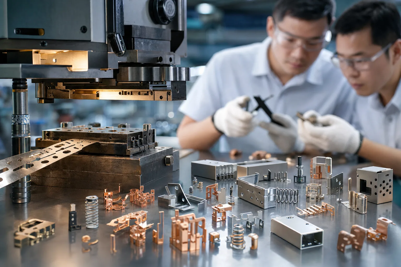
At Metal Stamping Parts, we manufacture electro-mechanical stamped components for automotive, industrial, consumer electronics, and telecommunications applications. This guide covers the materials, processes, tolerances, and quality considerations that define successful electro-mechanical stamping projects.
What Are Electro-Mechanical Stamped Components?
Electro-mechanical stamped parts are metal components that serve both structural and electrical functions within an assembly. They must meet mechanical requirements (strength, fatigue life, dimensional fit) while simultaneously delivering reliable electrical performance (conductivity, contact resistance, EMI shielding).
Electro-mechanical component stamping is the precision metal forming of parts that interface between electrical circuits and mechanical structures—including contacts, terminals, bus bars, shielding enclosures, and sensor mounts. These components require tight tolerances, specific material conductivity, and surface finish control to ensure reliable electrical performance over the product lifetime.
Common Electro-Mechanical Stamped Parts
- Electrical contacts and terminals: Power connectors, relay contacts, switch blades, PCB terminals
- Bus bars: High-current conductors for power distribution in switchgear, EVs, and industrial panels
- EMI/RFI shielding cans: Enclosures that block electromagnetic interference on PCBs
- Connector housings: Metal shells for multi-pin connectors in automotive and industrial applications
- Sensor brackets and mounts: Precision-formed parts that position sensors relative to target surfaces
- Lead frames: Semiconductor packaging components connecting chip die to external pins
- Battery contacts: Spring contacts and terminal plates for battery packs and consumer devices
- Heat sink mounting clips: Mechanical retention parts with thermal interface requirements
Materials for Electro-Mechanical Stamping
Material selection for electro-mechanical parts balances electrical conductivity, mechanical strength, formability, and cost. Unlike structural stamping where strength dominates, electro-mechanical applications often prioritize conductivity and surface characteristics.
Material Selection Guide
| Material | Conductivity (% IACS) | Tensile Strength (MPa) | Formability | Typical Applications |
|---|---|---|---|---|
| C11000 (ETP Copper) | 101 | 210–380 | Excellent | Bus bars, power contacts, grounding straps |
| C26000 (Brass 70/30) | 28 | 300–470 | Very Good | Connectors, terminals, receptacles |
| C51000 (Phosphor Bronze) | 15 | 325–700 | Good | Spring contacts, relay blades, switch parts |
| C72500 (Cu-Ni-Sn) | 11 | 450–850 | Fair | High-reliability connectors, aerospace terminals |
| Alloy 42 (Fe-Ni 42%) | 3 | 500–650 | Good | Lead frames, glass-to-metal seals |
| SPCC Steel | 10 | 270–410 | Excellent | Shielding cans, sensor brackets, chassis |
| Nickel 200 | 25 | 380–550 | Good | Battery contacts, corrosion-resistant terminals |
For most general-purpose electro-mechanical stamping, C26000 brass offers the best combination of conductivity, formability, and cost. For high-current applications, C11000 copper is preferred despite its lower strength. For spring-loaded contacts requiring fatigue resistance, C51000 phosphor bronze provides excellent elastic properties.
Plating and Surface Treatment
Electro-mechanical components almost always require surface plating for solderability, corrosion resistance, or contact resistance control:
- Tin plating: Excellent solderability, low cost. Thickness: 2–8 µm. Common for PCB terminals and general-purpose connectors.
- Nickel plating: Barrier layer for high-temperature applications. Thickness: 1–5 µm. Often used under gold plating.
- Gold plating: Lowest contact resistance, maximum corrosion resistance. Thickness: 0.05–1.25 µm (hard gold) or 0.025–0.05 µm (flash gold). Used for high-reliability connectors.
- Silver plating: High conductivity, good for high-current contacts. Thickness: 2–5 µm. Used in power connectors and bus bars.
- Zinc plating: Cost-effective corrosion protection for steel shielding cans. Thickness: 5–12 µm.
The Stamping Process for Electro-Mechanical Components
Electro-mechanical parts typically require progressive die stamping due to their small size, high volume, and complex geometry with multiple forming operations.
Progressive Die Stamping
Progressive dies are the workhorses of electro-mechanical stamping. A single die may contain 15–30 stations, each performing a specific operation:
- Pilot punching: Alignment holes for precise strip positioning
- Pre-forming: Partial bends or draws to prepare material for final forming
- Coining: Achieving precise flatness and thickness on contact surfaces
- Forming: Bending, drawing, or extruding features to final geometry
- Separation: Cutting the finished part from the carrier strip
Progressive die stamping uses a multi-station die in a single press, where the metal strip advances through each station with every press stroke. Each station performs a different operation—blanking, bending, coining, or forming—producing a finished part every cycle at speeds of 200–1,500 parts per minute.
Critical Process Controls
Electro-mechanical stamping requires tighter process controls than general stamping:
- Die clearance: Contact surfaces require clearance of 3–5% of material thickness per side. Too tight causes burrs; too loose degrades flatness.
- Coining pressure: Contact surfaces may require coining at 800–1,200 MPa to achieve Ra 0.4 µm surface finish and ±0.01 mm thickness tolerance.
- Strip orientation: Grain direction relative to bend lines affects springback and fatigue life. Strip must be oriented correctly in the die.
- Lubrication: Minimal lubricant is preferred for electro-mechanical parts to avoid contamination of contact surfaces. Dry film or micro-lubrication systems are common.
- In-die sensing: Vision systems and force monitors detect defects (cracks, missing features, dimensional drift) in real time without slowing production.
Tolerances and Specifications
Electro-mechanical components demand some of the tightest tolerances in stamping:
| Feature | Standard Tolerance | Precision Tolerance | Ultra-Precision |
|---|---|---|---|
| Contact tab width | ±0.05 mm | ±0.025 mm | ±0.010 mm |
| Terminal pitch | ±0.05 mm | ±0.03 mm | ±0.015 mm |
| Bend angle | ±1° | ±0.5° | ±0.25° |
| Flatness (contact area) | 0.05 mm/10mm | 0.02 mm/10mm | 0.01 mm/10mm |
| Burr height | ≤0.05 mm | ≤0.025 mm | ≤0.010 mm |
| Surface finish (coined) | Ra 0.8 µm | Ra 0.4 µm | Ra 0.2 µm |
Ultra-precision tolerances require carbide tooling, in-process gauging, and climate-controlled production environments. Not all parts need ultra-precision—standard tolerances are sufficient for most shielding cans and structural brackets.
Design Guidelines for Electro-Mechanical Parts
Engineers designing electro-mechanical stamped components should follow these guidelines to optimize manufacturability and performance:
Contact Design
- Contact beam length: Minimum 3× material thickness for adequate spring force and travel.
- Contact radius: 0.05–0.15 mm radius at contact tip to prevent stress concentration and improve mating durability.
- Retaining features: Barbs or interference fits should have 0.05–0.15 mm interference for secure press-fit assembly.
- Current-carrying capacity: Cross-sectional area determines ampacity. Rule of thumb: 10A per mm² for copper in still air.
Terminal and Connector Design
- Terminal pitch: Minimum 2× material thickness between adjacent terminals to prevent die breakage.
- Insertion force: Design press-fit terminals for 20–50N insertion force per contact—enough for retention, not so much as to damage the PCB.
- Selective plating: Gold plate only on the mating contact area to reduce cost. Nickel barrier layer on the solder tail.
Shielding Can Design
- Wall thickness: 0.2–0.5 mm typical for EMI shielding cans. Thicker walls improve shielding effectiveness but increase cost and weight.
- Ventilation holes: 1–2 mm diameter holes improve airflow while maintaining >20 dB shielding effectiveness.
- Seam design: Interlocking seams or soldered joints prevent RF leakage at corners.
Quality and Reliability Testing
Electro-mechanical stamped parts undergo rigorous testing beyond standard dimensional inspection:
Electrical Testing
- Contact resistance: Measured per EIA-364-06 or IEC 60512. Typical requirement: <10 mΩ for power contacts, <50 mΩ for signal contacts.
- Insulation resistance: >100 MΩ at 500V DC between adjacent contacts.
- Dielectric withstanding voltage: 1,000V AC for 60 seconds without breakdown (per IPC-A-610).
Mechanical Testing
- Insertion/withdrawal force: Measured per EIA-364-13. Cycle testing to verify contact spring life.
- Vibration testing: Per MIL-STD-202, Method 204. Contacts must maintain <10 mΩ resistance under vibration.
- Thermal cycling: −40°C to +125°C, 500 cycles minimum for automotive applications. Contact resistance must remain within specification.
- Salt spray testing: 48–96 hours per ASTM B117 for tin-plated parts, 500+ hours for nickel/gold.
Dimensional and Visual Inspection
- CMM measurement: Critical dimensions verified on coordinate measuring machines.
- Optical/vision inspection: 100% automated inspection for surface defects, burrs, and plating anomalies.
- Cross-section analysis: Metallographic cross-sections verify plating thickness, grain structure, and bond integrity.
Applications by Industry
Automotive Electronics
- EV battery terminal connectors (800V systems)
- ADAS sensor mounting brackets
- Onboard charger contacts
- CAN bus connector terminals
- Relay and contactor parts
Consumer Electronics
- USB-C and Lightning connector shells
- Battery spring contacts
- SIM card tray contacts
- Speaker grilles with EMI shielding
- Haptic motor mounting brackets
Telecommunications
- 5G antenna mounting hardware
- Fiber optic connector components
- PCB shielding enclosures
- Power distribution terminals
Industrial Controls
- PLC connector terminals
- Motor controller bus bars
- Circuit breaker contacts
- Industrial sensor housings
Frequently Asked Questions
What is the typical lead time for electro-mechanical stamping tooling?
Progressive die tooling for electro-mechanical components typically requires 4–8 weeks from design approval to first article parts. Complex multi-stage dies with in-die sensing may take 8–12 weeks. At Metal Stamping Parts, we deliver first article samples within 5 weeks for standard progressive dies and maintain in-house tooling capability for rapid modifications.
How does selective plating work for stamped terminals?
Selective plating applies precious metals (gold, silver) only to specific areas of a stamped part—typically the mating contact surface—while applying less expensive plating (tin, nickel) to the rest. This is achieved either by plating the flat strip before stamping (pre-plated strip) or by masking and plating after forming. Pre-plated strip is more common for high-volume production, offering lower cost and more consistent plating thickness.
What shielding effectiveness can stamped EMI cans achieve?
A properly designed stamped shielding can with continuous walls and soldered or gasketed seams provides 30–60 dB of shielding effectiveness from 100 MHz to 10 GHz. Ventilation holes reduce effectiveness by approximately 2–3 dB per hole depending on diameter and frequency. For applications requiring >60 dB shielding, two-piece cans with finger stock gaskets or board-level shielded compartments are used.
Can electro-mechanical parts be stamped and formed in a single die?
Yes. Progressive dies commonly combine cutting, forming, coining, and even assembly operations (such as inserting a contact into a housing) in a single die. In-die tapping, staking, and welding are also possible. This eliminates secondary operations, reduces handling damage, and lowers total cost per part. The trade-off is higher die complexity and cost.
What quality certifications are required for electro-mechanical stamping?
Requirements depend on the end application. ISO 9001 is the baseline for all suppliers. Automotive applications require IATF 16949. Aerospace and defense require AS9100 and often ITAR registration. Medical device components may require ISO 13485. For consumer electronics, many OEMs accept ISO 9001 with demonstrated PPAP capability. Metal Stamping Parts holds ISO 9001:2015 and IATF 16949:2016 certifications.
Conclusion
Electro-mechanical component stamping bridges the gap between electrical performance and mechanical precision. Whether you need high-current bus bars, spring-loaded contacts, or EMI shielding enclosures, progressive die stamping delivers the volume, consistency, and cost efficiency that these critical components demand.
Success in electro-mechanical stamping starts with the right material selection, follows with precision tooling design, and requires rigorous quality testing to ensure reliable performance over the product lifetime. Contact our engineering team at Metal Stamping Parts to discuss your electro-mechanical stamping requirements, request material recommendations, or get a production quote.