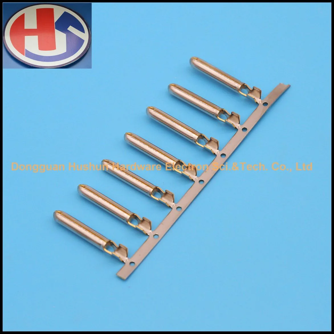
Electrical terminal stamping is the high-speed process of forming conductive metal contacts from strip material using progressive dies. Stamped terminal problems — from burrs and cracks to dimensional drift — can cause intermittent connections, field failures, and costly recalls in automotive, telecom, and consumer electronics assemblies. This guide catalogs the most common defects, explains their root causes, and provides actionable prevention strategies for every stage of the stamping and plating process.
Whether you source connector terminals from a contract stamper or run high-speed presses in-house, understanding these failure modes helps you tighten specifications, reduce scrap, and deliver reliable interconnects. Metal Stamping Parts Ltd produces millions of precision electrical contacts annually, and the lessons below reflect decades of production-floor experience.
Why Electrical Terminal Quality Matters
A single defective terminal in an automotive wiring harness can disable an entire circuit. In data-center power distribution, a poorly stamped bus bar contact can overheat and cause downtime. The stakes are high:
- Automotive: OEMs require <1 DPMO (defect per million opportunities) for safety-critical terminals.
- Telecom: Contact resistance must stay below 5 mΩ over the product lifetime.
- Consumer electronics: Miniaturized connectors demand ±0.01 mm positional accuracy.
Meeting these requirements starts with understanding the most common stamped terminal problems.
Common Defects in Stamped Electrical Terminals
The table below catalogs the ten most frequent defects seen in high-volume electrical terminal stamping, along with their root causes, prevention methods, and recommended corrective actions.
| # | Defect | Description | Root Cause | Prevention | Solution |
|---|---|---|---|---|---|
| 1 | Burr (excessive) | Sharp edge protrusions exceeding 0.02 mm on cut edges | Worn punch/die clearance, incorrect clearance setting, dull tooling | Maintain clearance at 5–7% of material thickness; schedule regrinding every 500K–1M hits | Sharpen or replace punch; verify clearance with optical measurement |
| 2 | Crack / fracture | Visible splits at bend radii or stress-concentration points | Material too hard, bend radius too tight, grain direction unfavorable | Select ductile temper (H condition for phosphor bronze); design bend radius ≥ 1× material thickness | Anneal bend zone; reorient part relative to grain direction |
| 3 | Dimensional deviation | Critical features (contact width, hole position) out of tolerance | Thermal expansion, material thickness variation, progressive die wear | Use SPC monitoring; control incoming material thickness to ±0.005 mm | Compensate die dimensions; install in-die sensors |
| 4 | Plating peeling / blistering | Tin, silver, or gold coating separates from base metal | Poor pre-plate cleaning, contaminated plating bath, inadequate underplate | Add nickel underplate (1.0–2.5 µm); maintain bath chemistry | Re-strip and re-plate; audit cleaning line |
| 5 | Twist / angular distortion | Terminal blade rotated out of plane after forming | Uneven material flow, asymmetric die geometry, strip misalignment | Balance forming stations; add anti-twist cams | Adjust die timing; add straightening station |
| 6 | Surface scratches | Linear marks on contact area from tooling contact | Debris on die surface, rough tool finish, improper material handling | Polish die surfaces to Ra ≤ 0.2 µm; use strip feeders with urethane rollers | Refinish die; add protective film on strip |
| 7 | Coining flash | Excess material extruded beyond coined feature boundaries | Excessive coining force, material too soft, worn coining punch | Optimize press tonnage; select correct temper | Reduce coining depth; replace worn punch |
| 8 | Spring-back (inconsistent) | Variable bend angles across a production lot | Material hardness variation, die temperature changes, lubricant inconsistency | Control incoming hardness to ±2 HRB; stabilize die temperature | Adjust bend angle compensation; standardize lubricant |
| 9 | Nesting / stacking defects | Terminals stick together in the output bin or on the strip | Burrs interlocking, static charge, inadequate stripping force | Optimize stripper spring force; add ionizer | Increase clearance; add air blast at die exit |
| 10 | Contact area contamination | Oil, fingerprint, or particulate on the mating surface | Stamping lubricant residue, handling without gloves | Use dry-film or evaporative lubricants; implement clean-room handling | Clean with IPA wipe; switch to post-stamp cleaning line |
Material Selection for Electrical Terminals
Choosing the right base material directly affects stampability, electrical performance, and long-term reliability. The table below compares the most widely used copper alloys in electrical terminal stamping.
| Alloy | UNS/CDA | Conductivity (% IACS) | Elastic Modulus (GPa) | Tensile Strength (MPa) | Typical Temper | Relative Cost | Best For |
|---|---|---|---|---|---|---|---|
| Phosphor Bronze | C51000 | 15 | 110 | 325–700 | H04 (hard) | Medium | General-purpose connectors, relays |
| Phosphor Bronze | C52100 | 13 | 110 | 450–800 | H08 | Medium-High | High-cycle contacts requiring fatigue life |
| Beryllium Copper | C17200 | 22 | 128 | 480–1,400 | TH04 | Very High | High-reliability aerospace, medical connectors |
| Brass (free-cutting) | C36000 | 26 | 97 | 340–470 | H02 | Low | Non-critical terminals, grounding clips |
| Brass (cartridge) | C26000 | 28 | 110 | 300–550 | H02 | Low-Medium | Deep-drawn shells, socket contacts |
| Nickel Silver | C75200 | 6 | 120 | 380–600 | H02 | Medium-High | Corrosion-resistant contacts, decorative terminals |
| Copper (ETP) | C11000 | 101 | 117 | 210–380 | H04 | Low | Bus bars, high-current power terminals |
Key selection criteria:
- Conductivity — Power terminals need >80% IACS; signal contacts can tolerate 10–30% IACS.
- Spring properties — Mating contacts require sustained deflection; phosphor bronze and BeCu excel.
- Formability — Complex geometries need elongation >10%; annealed tempers help.
- Stress relaxation — At elevated temperatures (85–150 °C), BeCu outperforms phosphor bronze by 2–3×.
For detailed guidance on electronics metal stamping capabilities, visit our dedicated page.
Plating Requirements Comparison
The plating system on an electrical terminal determines contact resistance, corrosion protection, solderability, and wear life. The table below compares the four most common plating options.
| Plating | Typical Thickness (µm) | Contact Resistance (mΩ) | Wear Life (mating cycles) | Corrosion Resistance | Solderability | Cost Level | Typical Application |
|---|---|---|---|---|---|---|---|
| Tin (mat or bright) | 2.5–8.0 | 10–15 | 50–100 | Moderate | Excellent | Low | Power connectors, automotive terminals |
| Silver | 1.0–5.0 | 1–3 | 100–500 | Moderate (tarnishes) | Good | Medium-High | High-current contacts, RF connectors |
| Gold (hard) | 0.5–1.25 | 1–2 | 500–10,000+ | Excellent | Good | Very High | Signal connectors, telecom, medical |
| Gold over nickel underplate | Au 0.75 / Ni 1.25–2.5 | 1–2 | 1,000–10,000+ | Excellent | Good | High | High-reliability data connectors |
| Palladium-Nickel + Gold flash | PdNi 0.5–1.0 / Au 0.05–0.1 | 2–5 | 500–5,000 | Very Good | Good | Medium | Cost-optimized high-reliability connectors |
Critical plating considerations:
- Nickel underplate (1.0–2.5 µm) is recommended for all gold-plated terminals — it acts as a diffusion barrier and improves wear resistance.
- Contact resistance should be measured per ASTM B539; values above 10 mΩ in signal circuits cause voltage drop issues.
- Porosity in thin gold deposits (<0.5 µm) allows base metal corrosion; specify porosity testing for harsh-environment applications.
High-Speed Stamping Precision Control (±0.01 mm Level)
Modern connector terminals are stamped at 300–1,500 strokes per minute. Achieving ±0.01 mm positional accuracy at these speeds requires tight control of every variable in the process.
Critical Control Factors
-
Die precision — Progressive dies for terminal stamping use carbide or powder-metal tooling with grinding tolerances of ±0.002 mm. Die sets must maintain parallelism within 0.005 mm across the full bolster area.
-
Press rigidity — High-speed presses with box-type frames and hydrostatic slide guides minimize deflection under load. Deflection at bottom dead center should not exceed 0.01 mm.
-
Strip feeding accuracy — Servo-driven roll feeds or gripper feeds achieve ±0.01 mm repeatability. Pilot pins in the die provide final location accuracy of ±0.005 mm.
-
Thermal management — Die temperature rises 5–15 °C during continuous running, causing thermal expansion. Precision dies incorporate cooling channels or are operated in temperature-controlled press rooms (20 ± 1 °C).
-
Material consistency — Incoming strip thickness variation must be controlled to ±0.005 mm (per ASTM B103 for phosphor bronze). Width variation should not exceed ±0.01 mm.
-
In-die sensing — Real-time monitoring with laser micrometers, vision cameras, and force sensors enables 100% inspection at line speed. Out-of-spec parts are automatically diverted.
Process Capability Targets
| Feature | Tolerance | Cpk Target | Measurement Method |
|---|---|---|---|
| Contact width | ±0.02 mm | ≥ 1.67 | Laser micrometer |
| Hole position | ±0.01 mm | ≥ 1.33 | Vision system |
| Terminal length | ±0.03 mm | ≥ 1.33 | In-die sensor |
| Bend angle | ±0.5° | ≥ 1.33 | Post-stamp gauge |
| Burrs | ≤ 0.02 mm | — | Optical / tactile |
Connector Terminal Design Best Practices
Well-designed terminals stamp consistently and perform reliably in the field. These terminal and contact stamping design principles reduce defects and lower per-part cost.
Geometry Guidelines
- Minimum bend radius: 1× material thickness for ductile alloys; 1.5× for hard tempers.
- Minimum web width: ≥ material thickness (preferably 1.5×) to prevent tearing.
- Hole-to-edge distance: ≥ 1.5× material thickness to avoid bulging.
- Tab aspect ratio: Length-to-width ≤ 3:1 to prevent buckling during forming.
- Relief notches: Add at the base of tabs to prevent crack propagation.
Electrical Performance Design
- Contact beam length: Longer beams reduce insertion force but increase contact resistance at high vibration.
- Normal force: 50–200 gf for signal contacts; 200–500 gf for power contacts.
- Multi-beam contacts: Two or more independent beams improve reliability by providing redundant contact points.
- Stress relief: Avoid sharp corners in the current path; radii reduce hot spots under high current.
DFM for High-Volume Production
- Design for progressive die stamping — avoid features requiring secondary operations.
- Standardize material thickness to common gauges (0.20, 0.25, 0.30, 0.40, 0.50 mm).
- Minimize the number of forming stations — each station adds die cost and tolerance stackup.
- Specify plating selectively — full-body plating is cheaper than selective plating for most applications.
Frequently Asked Questions
What causes excessive burrs in electrical terminal stamping?
Excessive burrs result primarily from worn punch edges, incorrect punch-to-die clearance, or material harder than the tooling design allows. When clearance exceeds 10% of material thickness, the sheared edge produces a rollover zone and burr that can exceed 0.05 mm. Preventive maintenance schedules should call for punch regrinding every 500,000 to 1,000,000 strokes, and incoming material hardness should be verified against the die design specification.
How do I choose between phosphor bronze and beryllium copper for connector terminals?
Phosphor bronze (C51000, C52100) is the default for most commercial connectors — it offers good conductivity (13–15% IACS), excellent fatigue life, and moderate cost. Beryllium copper (C17200) is the premium choice when you need higher conductivity (22% IACS), superior stress relaxation at elevated temperatures, or very high cycle life above 10,000 mating cycles. The trade-off is that BeCu costs 3–5× more than phosphor bronze and requires age-hardening heat treatment after forming.
What plating is best for automotive electrical terminals?
Mat tin plating (2.5–5.0 µm) over a nickel underplate (1.0–2.0 µm) is the standard for automotive terminals. Tin provides excellent solderability, adequate contact resistance (10–15 mΩ), and good corrosion protection in under-hood environments. For sealed connector cavities in critical safety systems (airbag, ADAS), some OEMs specify gold-over-nickel to ensure zero-failure contact reliability over 15-year vehicle life.
How accurate can high-speed stamping achieve for electrical terminals?
Modern progressive-die stamping on high-speed presses achieves ±0.01 mm positional accuracy for features like holes and contact edges, with Cpk values of 1.33 or higher. Terminal length tolerances of ±0.03 mm and bend angles within ±0.5° are routinely achievable at 600–1,200 SPM. Achieving these tolerances requires carbide tooling, servo feeds with pilot-pin registration, in-die sensing, and temperature-controlled press environments.
What is the most common cause of plating peeling on stamped terminals?
Plating peeling most often results from inadequate surface preparation before electroplating. Stamping lubricant residue, oxide films, and embedded abrasive particles prevent proper adhesion of the plated layer. Adding a nickel underplate (1.0–2.5 µm) between the base copper alloy and the final tin or gold topcoat dramatically improves adhesion and acts as a diffusion barrier. The cleaning line should include electro-cleaning, acid activation, and a rinse cascade before the nickel strike.
Conclusion
Electrical terminal stamping is a precision process where small deviations create significant reliability problems downstream. By understanding the root causes of common stamped terminal problems — burrs, cracks, plating defects, and dimensional drift — engineers can specify tighter incoming material controls, design stamping-friendly geometries, and select the right alloy and plating combination for each application.
If you need a stamping partner who understands connector terminal quality requirements, contact Metal Stamping Parts Ltd to discuss your next project. Our engineering team can help optimize your terminal design for high-volume production while meeting the tightest electrical and mechanical specifications.