
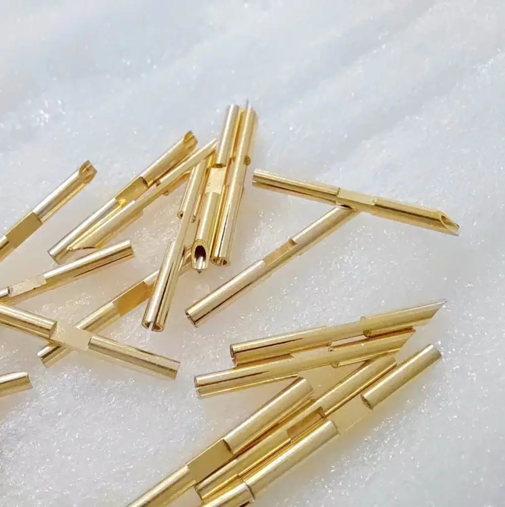
Short answer: precision small ການປັ໊ມໂລຫະ for electronics needs tight control of material temper, burr direction, flatness, plating, contact surfaces, spring behavior, cleanliness, and packaging. The parts may be tiny, but quote risk is high when drawings do not define function, assembly method, and inspection requirements.
This guide is for electronics buyers sourcing small stamped contacts, shields, springs, clips, brackets, lead frames, terminals, retainers, covers, and grounding parts. These parts often combine electrical, mechanical, cosmetic, and assembly requirements in one thin stamped component.
If you have a drawing or sample, send material, thickness, finish, critical dimensions, annual volume, and application notes through the RFQ form. For a complete package, use the ການປັ໊ມໂລຫະ RFQ checklist.
Small stamped electronics parts
Electronics ຊິ້ນສ່ວນປັ໊ມ often use copper alloys, brass, phosphor bronze, beryllium copper, stainless steel, aluminum, nickel silver, or plated steel. They may be used for conductivity, shielding, grounding, spring force, fastening, heat transfer, or mechanical support.
| Part type | Common function | RFQ concern |
|---|---|---|
| Connector contact | Electrical connection and spring force. | Material temper, plating, contact area, and force. |
| Grounding spring | Maintains electrical path between assemblies. | Spring height, fatigue, burr side, and plating wear. |
| EMI shield or finger | Shielding, grounding, and enclosure contact. | Flatness, wall height, corner damage, and packaging. |
| Mini bracket or retainer | Holds PCB, sensor, cover, cable, or module. | Hole position, bend angle, slot fit, and assembly stack. |
| Lead frame or tab | Electrical path, soldering, or component support. | Coplanarity, burrs, cleanliness, and reel/tray packing. |
Material and temper matter
For small electronic parts, the material is not just a cost line. Temper affects spring force, bend durability, contact reliability, and forming risk. Copper alloys may support conductivity. Phosphor bronze and beryllium copper may be used where spring properties matter. Stainless steel may be selected for corrosion or mechanical strength. Aluminum may support lightweight covers or thermal parts.
If the material is not fixed, tell the ຜູ້ສະໜອງ the function instead of leaving the choice open. Use the material selection guide and the copper alloy contact stamping guide when the part needs spring or electrical performance.
Tolerances, burrs, and small features
Small parts can make ordinary tolerances feel tight because a small shift may affect contact, insertion, soldering, or assembly. Hole position, slot width, tab height, bend angle, coplanarity, and contact area should be defined by function. Not every dimension needs a tight tolerance, but the important ones should be clear.
Burr direction can be functional. A burr on a contact edge may scrape plating. A burr on a PCB-facing edge may damage solder mask. A burr near an assembly slot may block insertion. Use the burr control guide and mark preferred burr side on the drawing when it matters.
Plating and contact surfaces
Plating may be used for conductivity, solderability, corrosion resistance, wear, or appearance. Tin, nickel, silver, gold, or other finishes may be considered depending on the application. The drawing should mark the contact zone, solder area, cosmetic side, masked area, and any surface where scratches are unacceptable.
Do not specify plating only by material name when contact resistance, solderability, or durability matters. Include the thickness, contact area, mating material, test expectation, and packaging requirement if known. Review the plating and passivation RFQ guide before quoting.
Cleanliness and handling
Small electronics parts may need controlled oil residue, no loose burrs, no fingerprints, no conductive contamination, or special cleaning before shipment. Cleaning requirements should be defined early because they affect process sequence, packaging, and cost.
Tell the ຜູ້ສະໜອງ whether the part will be soldered, bonded, assembled near optics, used in a sealed device, or handled by automated equipment. The packaging method should protect both part shape and surface cleanliness.
Prototype and production planning
Prototypes for small ຊິ້ນສ່ວນປັ໊ມ can confirm fit, insertion, contact, and assembly, but production may require ແມ່ພິມຕໍ່ເນື່ອງ stamping for stable volume and repeatability. A prototype made by laser cutting or simple tooling may not prove production burr direction, strip layout, carrier marks, or forming consistency.
If production volume is medium or high, compare tooling options with the ແມ່ພິມຕໍ່ເນື່ອງ cost guide and production ເວລານໍາສົ່ງ guide. For very small parts, handling and packaging can be as important as the stamping operation.
RFQ checklist for small electronics ຊິ້ນສ່ວນປັ໊ມ
- 2D drawing and 3D model with revision.
- Material grade, temper, thickness, and allowed substitutes.
- Electrical function: contact, grounding, shielding, soldering, or thermal transfer.
- Critical dimensions, contact zones, bend angles, coplanarity, and spring features.
- Finish or plating requirement, contact area, and surface restrictions.
- Burr direction, edge break, cleanliness, and no-loose-particle requirements.
- Prototype, pilot, annual volume, and production release schedule.
- Packaging method: bulk, counted bag, tray, reel, tube, or custom fixture.
Quality checks buyers should request
Dimensional inspection alone may not be enough. Depending on the part, request flatness, coplanarity, bend angle, spring height, insertion fit, plating appearance, contact resistance, solderability, burr check, or functional assembly check. For controlled programs, include first article inspection or PPAP/APQP requirements in the quote.
For quote support, send drawings, samples, target volume, and assembly notes through the RFQ form. Include photos of mating parts if the stamped part must contact, snap, solder, slide, or flex during use.
FAQ: small precision ການປັ໊ມໂລຫະ for electronics
What materials are common for small electronics ຊິ້ນສ່ວນປັ໊ມ?
Common options include copper alloys, brass, phosphor bronze, beryllium copper, stainless steel, aluminum, nickel silver, and plated steels.
Why is burr direction important?
Burr direction can affect contact surfaces, PCB safety, insertion force, plating wear, and assembly fit. Mark preferred burr side when it matters.
Can small ຊິ້ນສ່ວນປັ໊ມ be plated after stamping?
Often yes, but plating requirements should be defined before tooling because contact zones, masking, burrs, and packaging may affect the process.
Are prototypes enough to approve production?
Not always. Prototype methods may not match production tooling, strip layout, burr direction, or forming consistency. Confirm production samples separately.
What packaging is best for tiny ຊິ້ນສ່ວນປັ໊ມ?
It depends on geometry and assembly. Counted bags, trays, reels, tubes, or custom packaging may be needed to avoid mixing, bending, or contamination.
What should be sent for an RFQ?
Send drawings, material, thickness, finish, critical dimensions, annual volume, assembly function, cleanliness needs, and packaging requirements.