
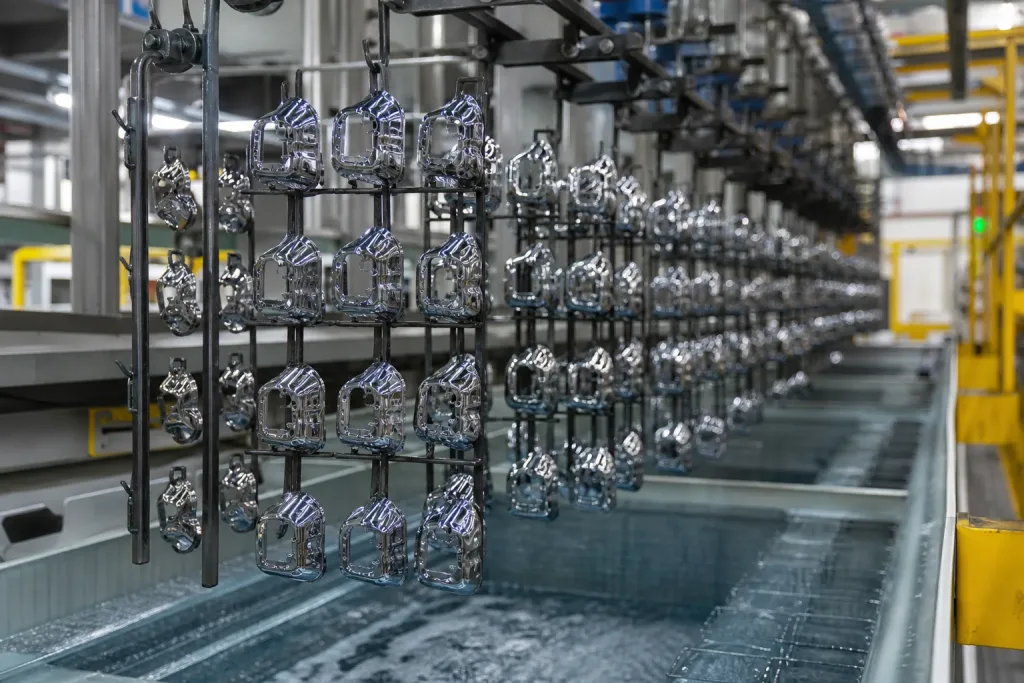
Short answer: Plating defect acceptance for bagian dicitak should define which defects are never acceptable, which are cosmetic only, and which depend on functional zones. Bare spots, blisters, peeling, thickness below minimum, corrosion, kontak-zone contamination, and solderability failures usually need stricter rules than small marks on non-functional areas.
Plating problems are expensive because they may appear after nyitak, deburring, cleaning, and outside processing. A drawing that says “tin plated” or “zinc plated” may not be enough. Buyers should define kontak zones, cosmetic zones, thickness readings, adhesion requirements, corrosion targets, and inspection conditions before quoting.
Use this guide with the plating and passivation RFQ guide, copper terminal plating selection guide, terminal plating thickness inspection guide, and surface finish inspection guide.
Biasa plating defects and acceptance logic
| Defect | Why it matters | Typical acceptance logic |
|---|---|---|
| Bare spot | Can expose base metal and reduce corrosion or kontak performance. | Usually reject on functional or protected zones; may need zone-based rules. |
| Blister or peeling | Shows poor adhesion and can flake during assembly or use. | Usually reject, especially on kontak, bend, or visible surfaces. |
| Thickness below minimum | May affect corrosion, solderability, wear, or electrical kontak. | Reject if below drawing or specification at defined measuring points. |
| Discoloration or stain | May be cosmetic only or may indicate process residue or corrosion. | Define visible zones, function risk, approved samples, and inspection lighting. |
| Rough deposit or nodules | Can affect mating, insertion, soldering, or packaging protection. | Reject on functional areas; review size and location on non-critical surfaces. |
Functional zones should be marked
A defect on a kontak surface is not the same as a small stain on a hidden carrier edge. Mark zones on the drawing or in the RFQ: kontak zone, solder zone, weld zone, cosmetic zone, non-critical edge, and handling area. This helps the panyadia quote inspection effort and avoid arguments after production.
For terminal and kontak parts, plating acceptance connects to conductivity, insertion wear, solderability, and corrosion. Pair this page with the terminal and kontak nyitak design guide and precision small electronics nyitak guide.
Inspection method changes the decision
Plating defects can be checked by visual inspection, microscope, XRF thickness reading, tape adhesion test, bend test, salt spray test, solderability test, or buyer-approved reference samples. The method should match the risk. A visual check cannot prove minimum thickness. A thickness reading may not prove appearance acceptance.
If plating thickness is critical, state the measuring location, sample size, minimum value, average value if used, and reporting requirement. For general appearance, define lighting, viewing distance, magnification if any, and acceptable reference samples.
Plating defects after forming or packaging
Some plating issues are not caused by the plating bath alone. Burrs, sharp edges, forming after plating, poor cleaning, fingerprints, part-to-part rubbing, moisture, and packaging pressure can all create visible or functional damage. The acceptance standard should connect plating with nyitak, cleaning, and packaging.
Use the cleanliness control guide and export packaging checklist when stains, water marks, fingerprints, or carton dust are part of the problem.
Plating defect RFQ checklist
- Base material, material thickness, plating type, underplate, topcoat, and passivation if used.
- Functional zones: kontak area, solder area, weld area, cosmetic face, bend area, and non-critical surfaces.
- Minimum plating thickness, measuring locations, XRF report need, and sample size.
- Rejectable defects: bare spots, peeling, blistering, corrosion, stains, rough deposits, nodules, or scratches.
- Cosmetic standard: viewing distance, lighting, magnification, approved samples, and defect size limits.
- Post-plating handling: cleaning, drying, packing, ESD, moisture control, and lot traceability.
- Failure photos, current panyadia reject reports, or customer complaint history if available.
When to request samples before approval
For visible or functional plated parts, approved samples can reduce disputes. Keep a golden sample and limit sample when possible. The limit sample should represent the edge of acceptance, not a perfect part. This is useful for stains, color variation, water marks, slight scratches, and other judgment-based findings.
If you need help defining plating defect acceptance for bagian dicitak, send the finish spec, drawing, critical zones, thickness requirement, photos, and report needs through the kontak page. Use the RFQ form to attach defect photos or current plating reports.
FAQ: stamped part plating defects
Are all plating stains rejectable?
No. Stains may be cosmetic or functional depending on location, cause, and customer standard. kontak, solder, and visible zones need clearer rules.
How should plating thickness be checked?
Define the measurement method, usually XRF for many plated bagian dicitak, plus measuring locations, sample size, minimum thickness, and report frequency.
Can packaging cause plating defects?
Yes. Moisture, rubbing, paper dust, fingerprints, pressure, and poor drying can create stains, scratches, corrosion, or residue after plating.
What should buyers send for plating defect review?
Kirim the drawing, finish spec, functional zones, cosmetic standard, thickness requirement, inspection method, photos, and current reject history.