
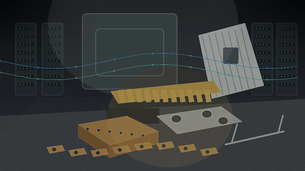
Short answer: stamped EMI/RF spring contacts are formed metal parts that keep conductive contact between shields, boards, covers, frames, or housings. A good design balances spring force, contact resistance, plating, burr direction, height, fatigue life, and assembly method. For an RFQ, send drawings, material, thickness, finish, contact height, compression range, tolerance, and annual volume.
For a quote, send your drawing and application notes through the RFQ form. For related shielding topics, review EMI shielding ਸਟੈਂਪ ਕੀਤੇ ਭਾਗ, stamped grounding clips, and electrical connector shield stamping.
Where EMI/RF spring contacts are used
Stamped EMI/RF contacts are used where one conductive surface must touch another after assembly. Common examples include shield cans, PCB grounding points, telecom modules, sensor covers, battery housings, metal enclosures, connector shells, antennas, and electronic frames. The contact may be a single spring finger or a repeated pattern along a shield edge.
The important question is not only whether the part can be stamped. The ਸਪਲਾਇਰ must understand the working height, compression travel, mating surface, required force, plating, and how the part will be installed. A spring that is too soft may lose contact. A spring that is too stiff may damage a board, cover, or plastic housing.
Material selection for spring contact behavior
Material choice depends on conductivity, spring recovery, corrosion exposure, forming severity, and cost. Phosphor bronze is often used where formability and spring properties must be balanced. Beryllium copper can provide stronger spring recovery and fatigue performance when the application justifies the material and process control. Stainless steel may work for corrosion resistance or mechanical spring needs, but it is not as conductive as copper alloys unless the design and plating compensate for that.
For battery, terminal, and connector contacts, buyers may also compare copper alloys, brass, and nickel-plated materials. If the electrical path is critical, define the mating surface and contact resistance requirement if known. For alloy comparison, see phosphor bronze and beryllium copper contact stamping.
Geometry, thickness, and contact force
Spring force is controlled by material, thickness, beam length, bend radius, working height, and forming accuracy. Increasing thickness can raise force, but it may also increase insertion load, bend stress, and tooling difficulty. A longer beam can reduce stress, but it needs more space. A coined or dimpled contact point can localize contact pressure, but it also adds tooling and inspection requirements.
Drawings should define free height, compressed height, contact tip location, beam width, mounting holes or tabs, datum features, and burr side. Burr direction matters because a rough edge can scratch a plated mating surface, damage a PCB pad, or create unstable contact. If the part slides during assembly, define the functional wipe surface clearly.
EMI and RF design considerations
For EMI shielding and RF continuity, the contact is part of an electrical path. Buyers should define whether the part provides grounding, shielding continuity, antenna contact, board-to-cover contact, or frame-to-frame contact. Contact pitch, compression consistency, oxide buildup, and plating choice can all affect performance.
For high-frequency or sensitive applications, the product engineering team usually validates electrical behavior. The stamping ਸਪਲਾਇਰ controls dimensions, material, finish, forming repeatability, edge quality, and packaging. If the contact is used with a shield can or enclosure, include an assembly drawing so the grounding path can be reviewed.
Plating and surface treatment
Finish selection depends on contact resistance, corrosion risk, wear, solderability, and cost. Tin plating is common for many grounding and contact parts. Nickel may be used as a barrier layer or for wear and corrosion control. Gold may be specified for low-current signal contacts, sensitive RF contact points, or corrosion-sensitive assemblies, but selective plating should be reviewed when only the contact area needs the premium finish.
Plating sequence matters. Pre-plated strip can reduce process cost, but cut edges may expose base metal. Post-plating can cover more surfaces, but formed geometry and nesting must be controlled. For finish planning, use the ਮੈਟਲ ਸਟੈਂਪਿੰਗ plating and passivation RFQ guide.
Tooling and production method
Low-volume contacts may start with prototype tooling or simple forming fixtures. Production parts often move to ਪ੍ਰੋਗਰੈਸਿਵ ਡਾਈ stamping so blanking, piercing, forming, coining, and cutoff run in sequence. Progressive tooling helps when contact force, burr direction, and carrier strip handling must stay consistent.
Features that deserve early DFM review include narrow beams, tight inside radii, small lances, coined tips, close holes, carrier break points, and plating-sensitive surfaces. For broader process context, see custom ਮੈਟਲ ਸਟੈਂਪਿੰਗ and products and services.
Inspection and packaging
Useful inspection points include material certificate, thickness, formed height, working height, contact tip position, plating thickness, burr side, visual surface condition, and contact force at the specified compression. A simple height gauge or go/no-go fixture can be more meaningful than measuring every edge dimension.
Packaging should protect formed beams. Small spring contacts can tangle, flatten, or scratch each other if bulk packed without control. Depending on the shape, trays, reels, small bags, or layered packaging may be needed. If parts feed into an assembly process, state orientation and quantity per package.
What to include in the RFQ
- 2D drawing and 3D file with revision level.
- Material grade, thickness, temper, and acceptable alternatives.
- Free height, working height, compression range, and contact force target if known.
- Plating stack, contact surface, burr direction, and cleanliness needs.
- Assembly method: soldered, clipped, inserted, riveted, welded, or manually installed.
- Prototype quantity, annual volume, packaging method, inspection requirements, and target ਲੀਡ ਟਾਈਮ.
Send your stamped EMI/RF spring contact drawings through the RFQ form. If the design is still open, include the mating surface, available space, shielding requirement, and current issue such as weak grounding, corrosion, high insertion force, or unstable contact.