
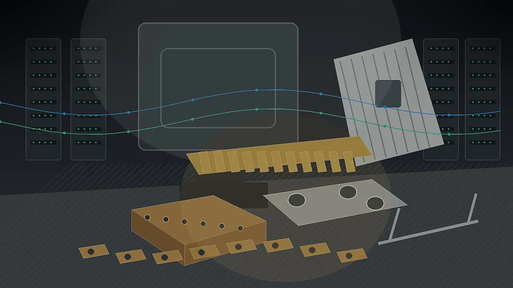
Short answer: stamped electrical connector shields are thin metal enclosures formed to wrap around connector bodies or pin fields for EMI/RFI protection, grounding, and mechanical retention. They are typically made from stainless steel, tin-plated steel, brass, or copper alloys with spring finger features for reliable ground tuntuɓa.
This guide is for connector design engineers, RF engineers, and sourcing teams who need stamped EMI shields for USB, HDMI, RJ45, motoci connectors, 5G base-station connectors, backplane connectors, and telecom or datacom interconnect systems. The shield must provide consistent electrical tuntuɓa, survive mating cycles, and meet assembly tolerances.
Aika drawings with material, plating, shield dimensions, tuntuɓa finger requirements, and assembly constraints through the RFQ form. For related parts, see terminal and tuntuɓa bugawa design guide and the EMI shielding sassan da aka buga guide.
gama gari connector shield applications
- USB-C, HDMI, DisplayPort, and RJ45 connector shields for consumer and industrial electronics.
- motoci connector shields for ADAS, infotainment, and powertrain control modules.
- 5G and telecom connector shields for base station, antenna, and backplane interconnects.
- Backplane connector shields for server, storage, and networking equipment.
- Board-to-board and mezzanine connector shields for compact electronic assemblies.
- RF coaxial connector shields and grounding springs for signal integrity applications.
For circuit-level EMC parts, see stamped heat sinks and thermal parts guide for related thermal management components.
Materials for stamped connector shields
| Material | EMI performance | Spring properties | Typical plating |
|---|---|---|---|
| Stainless steel 301 (full hard) | Good (magnetic) | Excellent | None or tin |
| Tin-plated steel (SPTE/CRS) | Good (magnetic) | Moderate | Tin pre-plated |
| Brass C260 (half-hard) | Moderate (non-magnetic) | Good | Tin, nickel, or silver |
| Phosphor bronze C510 | Moderate (non-magnetic) | Excellent | Tin or silver |
| Copper C110 (for gaskets) | Excellent (non-magnetic) | Poor | Tin or none |
| Beryllium copper C172 | Moderate (non-magnetic) | Mafi kyawun (high fatigue) | Tin, nickel, or gold |
For more on tuntuɓa materials and spring properties, see phosphor bronze and beryllium copper tuntuɓa bugawa.
Spring finger design
The spring fingers of a connector shield must provide consistent tuntuɓa pressure against the mating connector body or chassis ground across the product life. Key design factors include:
- Finger length and width. Longer, narrower fingers deflect more for a given force, which is useful for tolerance accommodation. Shorter, wider fingers provide higher force at a given deflection, which helps in high-vibration environments.
- Bend radius. Tight radii on spring fingers can cause stress concentration. Minimum bend radius of 1.0 to 1.5 times material thickness is typical for stainless steel. For more design rules, see the bugun karfe part design guide.
- tuntuɓa surface. The tip of each spring finger often has a coined or formed dome, ramp, or flat surface that contacts the mating shield or ground trace. Coining the tip increases tuntuɓa area and reduces wear.
- Venting and forming direction. The shield may include slots or louvers that are formed inward or outward. The forming direction must not interfere with the connector body insertion path.
For deeper spring tuntuɓa design, see stamped metal clips and spring clips guide.
Tolerances for connector shields
Connector shield tolerances depend on the mating connector interface, assembly method, and whether the shield uses compliant or interference-fit features:
- Overall shield envelope: ±0.10 mm for precision applications, ±0.20 mm for commercial.
- Spring finger position: ±0.08 mm for high-speed signals where impedance matters.
- Spring finger deflection gap: ±0.05 mm after forming (controlled by tooling).
- Hole and slot positions: ±0.10 mm.
- Burr height: 0.05 mm max for tuntuɓa fingers, 0.08 mm acceptable for non-tuntuɓa surfaces.
- Shell flatness after forming: 0.10 mm per 25 mm for pick-and-place compatibility.
For comprehensive tolerance data, see bugun karfe tolerances guide.
Plating and surface finish
Connector shields are plated to prevent corrosion, improve ground tuntuɓa resistance, and meet appearance or solderability requirements:
- Tin plating — most common for consumer electronics shields. Matte tin preferred to reduce whisker risk. 2 to 5 microns typical.
- Nickel underplate + tin — for shields soldered to PCBs; nickel prevents copper migration during reflow.
- Silver plating — for RF shields where surface conductivity affects insertion loss and return loss. 2 to 4 microns typical.
- Gold plating over nickel — for high-reliability or low-signal-level connectors where oxide-free tuntuɓa is critical.
- Tin-zinc alloy — for motoci shields with galvanic compatibility requirements.
Selective plating is common for connector shields — only the spring finger tuntuɓa areas and solder tails are plated, while the rest of the shield remains bare or with minimal flash. For more on finishes, see bugun karfe plating and passivation RFQ guide.
Assembly and manufacturing considerations
SMT compatibility. Most connector shields are designed for surface-mount reflow soldering. Key SMT requirements include: flatness within 0.10 mm for pick-and-place, solder tail design for consistent paste deposition, and high-temperature material stability through reflow.
Shield orientation. The shield must be inserted or assembled in only one correct orientation. Include polarization features such as corner notches, keying slots, or asymmetrical tab patterns to prevent misassembly.
Ventilation and drain holes. Connector shields often include vent holes or drain slots that allow solder flux vapor or moisture to escape during reflow. Without vents, the shield can act like a sealed chamber, causing solder defects or corrosion inside the shield cavity.
For more on packing, see bugun karfe packaging and shipping guide.
RFQ checklist for connector shields
- Drawing with flat pattern, formed shield views, and spring finger details.
- Material: grade, temper, thickness, and plating spec.
- Shield envelope dimensions and tolerances (length, width, height, flatness).
- Spring finger count, position, deflection, tuntuɓa force, and fatigue life requirements.
- Annual volume and order quantity.
- Assembly method: SMT reflow, through-hole, press-fit, or hand solder.
- Plating requirements: full or selective; material, thickness, and zones.
- Packaging: tape-and-reel for SMT, or trays/tubes.
- Testing: insertion force, tuntuɓa resistance after environmental cycling, salt spray, or RoHS/REACH compliance.
Submit your shield drawing through the RFQ form. For general RFQ preparation, see the bugun karfe RFQ checklist.